- English
- Español
- Português
- русский
- Français
- 日本語
- Deutsch
- tiếng Việt
- Italiano
- Nederlands
- ภาษาไทย
- Polski
- 한국어
- Svenska
- magyar
- Malay
- বাংলা ভাষার
- Dansk
- Suomi
- हिन्दी
- Pilipino
- Türkçe
- Gaeilge
- العربية
- Indonesia
- Norsk
- تمل
- český
- ελληνικά
- український
- Javanese
- فارسی
- தமிழ்
- తెలుగు
- नेपाली
- Burmese
- български
- ລາວ
- Latine
- Қазақша
- Euskal
- Azərbaycan
- Slovenský jazyk
- Македонски
- Lietuvos
- Eesti Keel
- Română
- Slovenski
- मराठी
- Srpski језик


Čína Oplatka výrobce, dodavatel, továrna
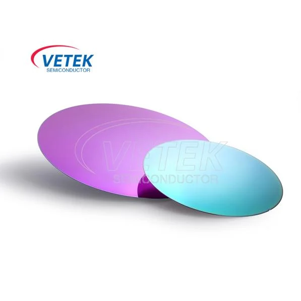
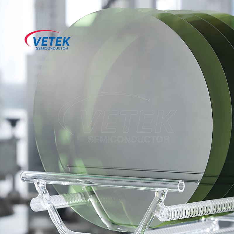
Wafer Substrate is a wafer made of semiconductor single crystal material. The substrate can directly enter the wafer manufacturing process to produce semiconductor devices, or it can be processed by epitaxial process to produce epitaxial wafers.
Wafer Substrate, as the basic supporting structure of semiconductor devices, directly affects the performance and stability of the devices. As the "foundation" for semiconductor device manufacturing, a series of manufacturing processes such as thin film growth and lithography need to be carried out on the substrate.
Summary of substrate types:
1. Single crystal silicon wafer: currently the most common substrate material, widely used in the manufacture of integrated circuits (ICs), microprocessors, memories, MEMS devices, power devices, etc.;
2. SOI substrate: used for high-performance, low-power integrated circuits, such as high-frequency analog and digital circuits, RF devices and power management chips;
3. Compound semiconductor substrates: Gallium arsenide substrate (GaAs): microwave and millimeter wave communication devices, etc. Gallium nitride substrate (GaN): used for RF power amplifiers, HEMT, etc. Silicon carbide substrate (SiC): used for electric vehicles, power converters and other power devices Indium phosphide substrate (InP): used for lasers, photodetectors, etc.;
4. Sapphire substrate: used for LED manufacturing, RFIC (radio frequency integrated circuit), etc.;
Vetek Semiconductor is a professional SiC Substrate and SOI substrate supplier in China. Our 4H semi-insulating type SiC substrate and 4H Semi Insulating Type SiC Substrate are widely used in key components of semiconductor manufacturing equipment.
Vetek Semiconductor is committed to providing advanced and customizable Wafer Substrate products and technical solutions of various specifications for the semiconductor industry. We sincerely look forward to becoming your supplier in China.
- View as

4° mimo osu SiC Wafer typu p
VeTek Semiconductor je profesionální čínský výrobce SiC waferu typu p se 4° mimo osu, substrátu SiC typu 4H N a substrátu SiC typu 4H Semi Insulating. Mezi nimi 4° mimo osu typu p SiC Wafer je speciální polovodičový materiál používaný ve vysoce výkonných elektronických zařízeních. VeTek Semiconductor se zavazuje poskytovat pokročilá řešení pro různé produkty SiC Wafer pro polovodičový průmysl. Upřímně se těšíme na vaši další konzultaci.
Přečtěte si víceOdeslat dotaz
4H SiC substrát typu N
Jako profesionální výrobce a dodavatel SiC substrátu 4H typu N v Číně se Vetek Semiconductor 4H substrát SiC typu N snaží poskytovat pokročilé technologie a produktová řešení pro polovodičový průmysl. Náš 4H N-type SiC Wafer je pečlivě navržen a vyroben s vysokou spolehlivostí, aby splnil náročné požadavky polovodičového průmyslu. Uvítáme vaše další dotazy.
Přečtěte si víceOdeslat dotaz
4H poloizolační typ SiC substrát
Vetek Semiconductor je profesionální výrobce a dodavatel 4H poloizolačního SiC substrátu v Číně. Náš 4H poloizolační SiC substrát je široce používán v klíčových součástech zařízení na výrobu polovodičů. Společnost Vetek Semiconductor se zavázala poskytovat pokročilá řešení 4H poloizolačních produktů SiC pro polovodičový průmysl. Vítáme vaše další dotazy.
Přečtěte si víceOdeslat dotaz
Jako profesionální výrobce a dodavatel Oplatka v Číně máme vlastní továrnu. Ať už potřebujete přizpůsobené služby, které splňují specifické potřeby vašeho regionu, nebo si chcete koupit pokročilé a odolné Oplatka vyrobené v Číně, můžete nám zanechat zprávu.